The emerging role of SRAM-centric chips in AI inference
- Published on
- Authors

- Name
- Natalie Serrino

- Name
- Zain Asgar
The emerging role of SRAM-centric chips in AI inference
tl;dr: In this post, we'll discuss the major differences between GPUs and SRAM-centric accelerators (e.g. Cerebras, Groq, and d-Matrix), explaining why near-compute memory versus far-compute memory is the key tradeoff being made by these architectures, and what this means for inference workloads.
It's been a notable few months for SRAM-centric AI accelerators: NVIDIA licensed Groq's IP for $20B in December, and Cerebras announced a 750 MW deal to run OpenAI inference workloads. These are major proof points for SRAM-centric architectures (such as Cerebras, Groq, and d-Matrix), which claim to offer significant latency and throughput advantages over traditional GPUs.
With top labs increasingly investing in inference speed and throughput, SRAM-centric accelerators are positioned to capture a meaningful share of the market. As we'll discuss, both SRAM-centric chips and GPUs excel at different types of tasks, and understanding those tradeoffs is key to predicting where the industry might be headed.
At Gimlet, we run our own multi-silicon inference cloud, deploying both traditional GPUs and SRAM-centric chips. Our software orchestration slices and maps inference workloads to the optimal hardware, and that experience has given us a practical view of where each architecture sits.
In this post, we'll share some of our learnings and discuss:
- The physical differences between SRAM and HBM, and why they matter for inference
- How those differences shape chip architecture (and why the most important tradeoff is actually near-compute vs far-compute memory)
- Why arithmetic intensity determines which approach wins, and the impact of these design choices on inference performance
- Predictions for how the industry will converge based on current trends
One of our core takeaways is that the working set size in the workload determines the arithmetic intensity, which in turn determines whether near-compute memory or far-compute memory is the right choice. SRAM is a hot topic in AI accelerators right now, but it's one implementation of a deeper architectural decision. As we'll discuss at the end of the post, we expect new memory designs to fill in some of the roles currently occupied by both SRAM and HBM.
The physical differences between SRAM and DRAM
SRAM-centric architectures can be faster than GPUs because accessing SRAM is faster than accessing HBM, which speeds up the entire workload. SRAM is faster than HBM (which is a form of DRAM) for 2 reasons:
- SRAM reads are physically faster than DRAM reads.
- SRAM lives on-chip with the compute cores, offering significant locality advantages, whereas HBM lives off-chip.
SRAM cells are designed to be extremely low latency, but they use more transistors per bit than DRAM cells, which are simpler and more spatially compact. Compare a single DRAM cell (left) to a single SRAM cell (right):
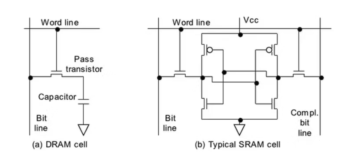
Image source. DRAM cell (left) vs SRAM cell (right). The DRAM cell is more spatially compact, and the SRAM cell is lower latency.
- SRAM uses 6 transistors for each bit, containing two inverters (2 transistors each) in a cross-coupled orientation. The bit state is always actively held, so reads are fast (~1 ns) and non-destructive.
- DRAM uses 1 transistor and 1 capacitor to hold each bit. The capacitor storing the bit is slower to read from (~10-15 ns) than an active bit state like SRAM.
The benefit of DRAM is that its tiny physical size means that you can get very high memory density, whereas SRAM has a larger footprint but is faster. Another difference is SRAM can be built on-chip with the same process, whereas DRAM requires a specialized process and must be off-chip.
In the GPU memory hierarchy, the faster, on-die memory levels are therefore SRAM whereas the slower, denser, off-chip memory levels are DRAM. Jarmusch et al estimated the access time in cycles for each level for the H100:
| Memory Level | Memory Type | Access Time | Memory size |
|---|---|---|---|
| Registers | SRAM | <1 ns | 256 kB/SM |
| Shared Memory | SRAM | ~20 ns | Total of 256 kB/SM shared with L1 Cache |
| L1 Cache | SRAM | ~20 ns | Total of 256 kB/SM shared with Shared Memory |
| L2 Cache | SRAM | 115 - 200 ns | 50 MB |
| VRAM (HBM3) | DRAM | 375 - 500 ns | 80 GB |
We need these different levels of the hierarchy because the different types of memory exist on a Pareto curve - SRAM is faster but expensive, whereas DRAM is slower but cheaper. The chip die only has so much space for SRAM, and there's also an opportunity cost of spending die area on SRAM rather than compute.
The H100 has 50 MB in SRAM, rising to 126 MB for the B200, whereas SRAM-centric architectures invest more heavily:
| Chip | Die area | Process Node | SRAM Capacity | SRAM/mm^2 per chip |
|---|---|---|---|---|
| B200 (dual-die) | ~1600 mm² | 4 nm | 126 MB L2 | 0.08 MB/mm² |
| Groq LPU v1 | 725 mm² | 14 nm | 230 MB | *0.32 MB/mm² |
| d-Matrix Corsair | 400 mm² | 6 nm | 256 MB | 0.64 MB/mm² |
| Cerebras WSE-3 | 46255 mm² | 5 nm | 44 GB | 0.97 MB/mm² |
B200: source, source, source. Groq: source, source. d-Matrix: source, source. Cerebras: source, source.
* Note that Groq LPU v1 uses a 14 nm process, whereas the other chips use smaller processes.
The impact of memory placement on chip architecture and programming model
SRAM-centric chips like Cerebras, d-Matrix, and Groq are not just GPUs with sized-up caches. They take on a fundamentally different strategy in addressing the same memory scaling tradeoff that GPUs solve with the GPU memory hierarchy. Both architectures have to address the same central tension:
- Far-memory compute like DRAM offers effectively unlimited capacity, but the memory bandwidth delivered to the chip scales with the perimeter of the chip, whereas compute scales with the area of the chip.
- With near-memory compute like SRAM, memory bandwidth scales better with chip size, but it is strictly limited by chip size and requires sacrificing compute capacity. This memory bandwidth advantage only applies to data that can fit on chip.
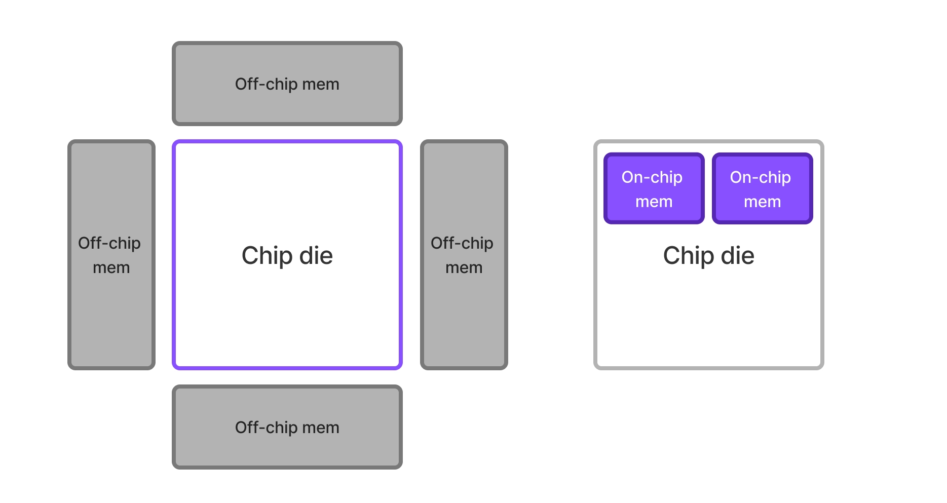
Comparison of off-chip memory vs on-chip memory: Off-chip memory bandwidth scales O(1/sqrt(N)) with chip area, whereas on-chip memory bandwidth scales closer to O(1) with chip area but is fundamentally capped by total chip size and zero-sum with compute capacity.
As the CTO of d-Matrix noted, "Industry benchmarks show that compute performance has grown roughly 3x every two years, while memory bandwidth has lagged at just 1.6x.".
GPUs handle this scaling challenge by defining memory tiers, where expensive memory fetches are avoided through caching and reuse of data. SRAM-centric architectures instead sacrifice compute in favor of a larger, flatter memory hierarchy. Which approach wins for a given workload depends on whether its working set is well matched to a traditional cache hierarchy, or if it's better served by a larger pool of working memory.
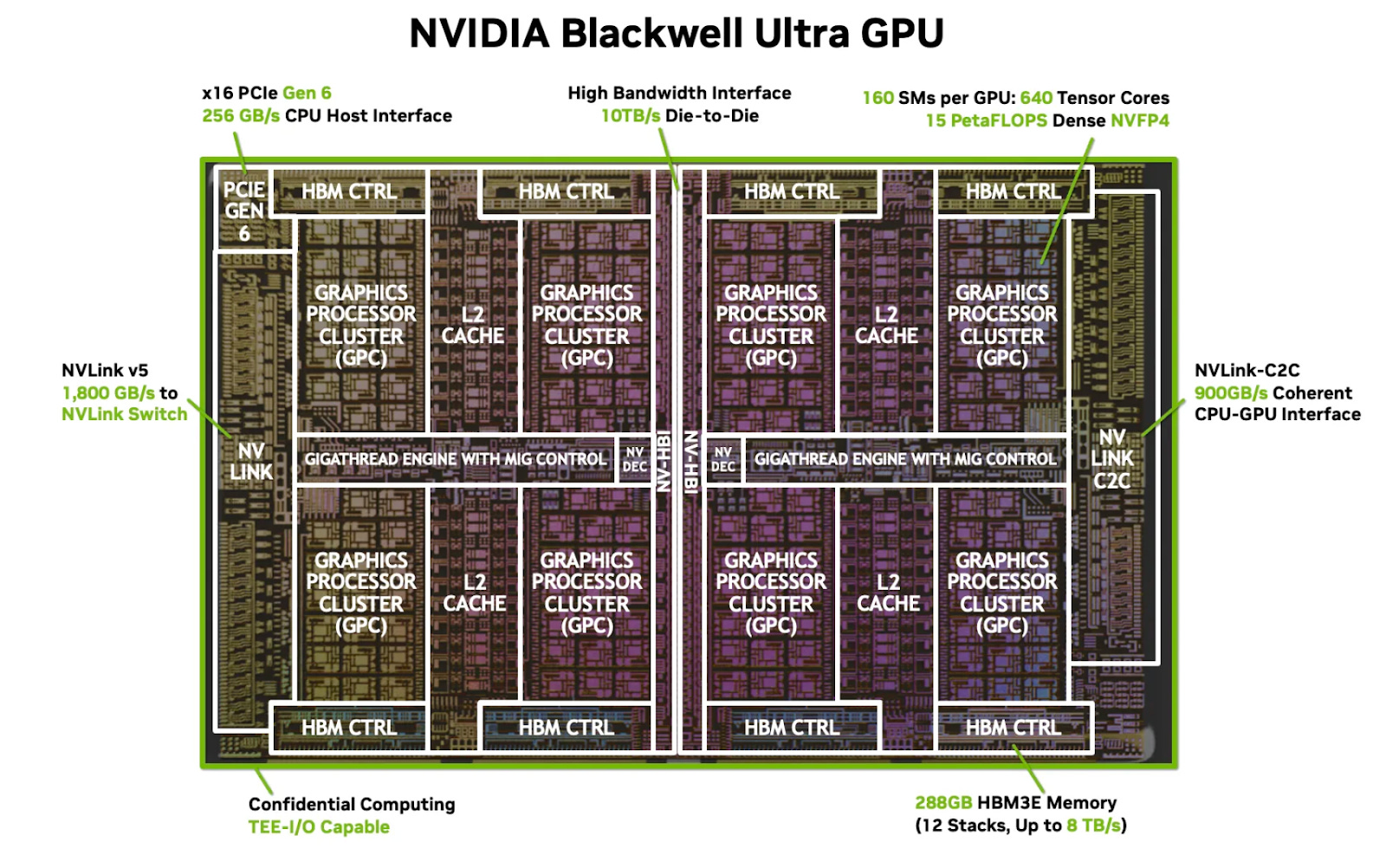
Image source. View of the NVIDIA Blackwell GPU, which has a traditional cache-based memory hierarchy.
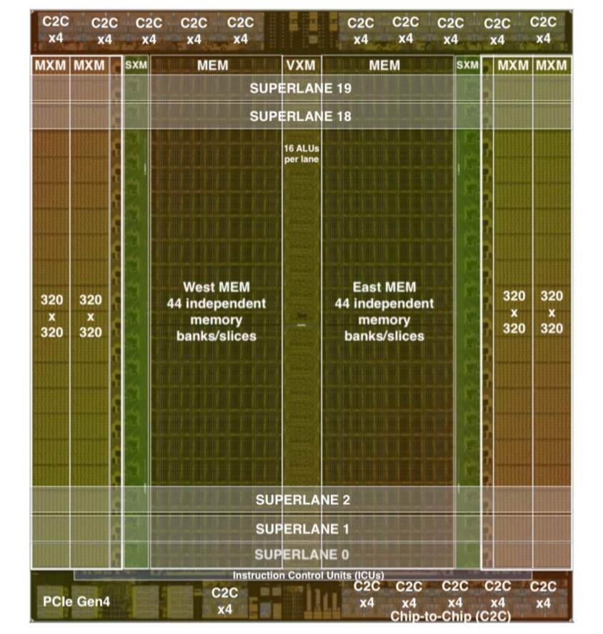
View of Groq's LPU (source), showing its superlane architecture with SRAM (West/East MEM) and compute units.
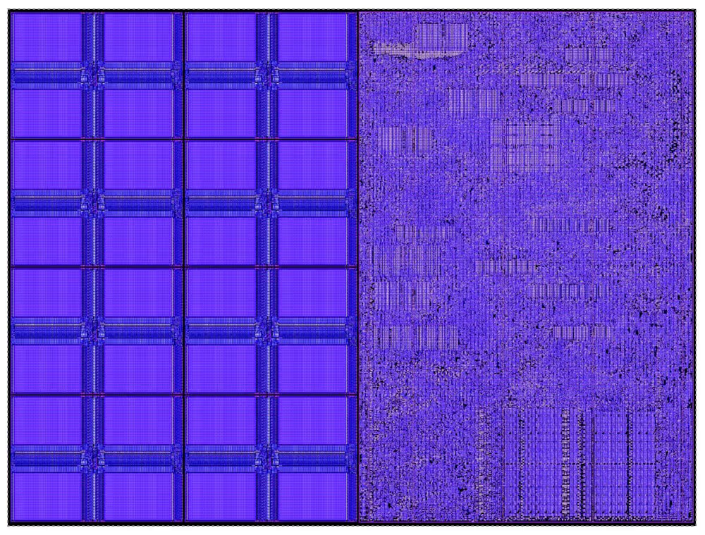
Image source. View of a single Cerebras core, which devotes about 50% of its area to memory (left).
High-performance GPU programs minimize data movement, tiling the data strategically to fit on device and maximize data reuse.
GPUs perform very well when data reuse is high, and the full benefit of the dense compute can be used. Workloads are characterized based on their arithmetic intensity, which measures the amount of work an algorithm does per byte of memory. Higher arithmetic intensity workloads tend to be faster because they can leverage the full power of the compute, whereas lower arithmetic intensity workloads are bottlenecked on data movement.
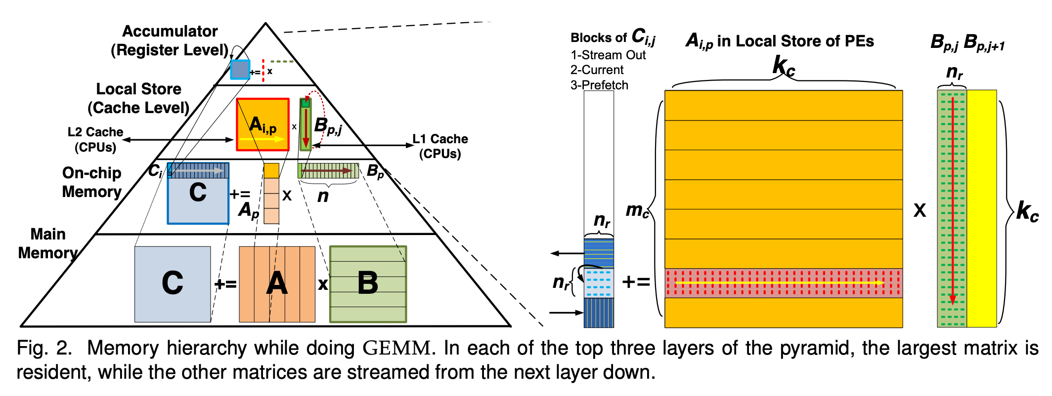
How a matrix multiplication gets mapped across the layers of the memory hierarchy in a GPU. Source: Pedram et al.
SRAM-centric architectures have a fundamentally different programming model. Chips like Cerebras, Groq, and d-Matrix differ significantly in their approach, but a few common trends fall out of the fundamental decision to leverage a flatter, SRAM-centric memory system.
First, data placement becomes a physical mapping problem. On a GPU, while shared memory is manually managed, caches are typically managed automatically by the hardware.
On SRAM-centric architectures, the memory is highly distributed throughout the chip, and there is no abstraction like a memory hierarchy hiding the exact physical layout. Software explicitly decides where the data lives, with the goal of ensuring it's optimally placed for compute.
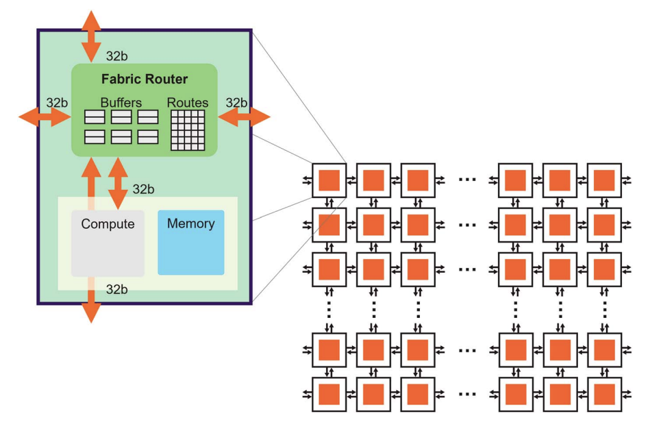
High-level view of the Cerebras architecture (source). Because data is distributed throughout the fabric of cores, it must be explicitly placed and optimized at the software level.
The programming challenge in SRAM-centric architectures is not tiling the data to fit into cache and maintain high compute intensity, but rather fitting and distributing the workload onto the chip's available memory capacity. On a GPU, model weights live in HBM and stream through the cache hierarchy. On SRAM-centric architectures, weights are stored directly on-chip to maximize the memory bandwidth advantage. However, as we already know, the total available on-chip memory is fundamentally constrained by chip size. Even Cerebras, the largest SRAM-centric chip which uses an entire wafer, "only" has 44 GB of SRAM storage, so weights for large models need to be distributed across multiple chips.
Because SRAM-centric chips trade away compute capacity for more on-chip memory, they perform best at workloads that are memory bandwidth-bound where large amounts of data need to be streamed with minimal reuse.
Why SRAM-centric architectures favor inference workloads
GPUs dominate at training workloads because training has high arithmetic intensity. In both training and inference, weights are loaded in from HBM to the chip's SRAM in tiles (subsections). Each weight tile is multiplied with the input tokens and then the next tile is loaded in.
For both prefill and training, many input tokens are processed at the same time. That means the load of a given tile of weights can be amortized across a long input sequence, creating very high arithmetic intensity (large amounts of compute operations relative to memory operations).
Decode, on the other hand, is auto-regressive. Each token has to be processed fully before the computation for the next one can begin. That means that we have to load each of the weight tiles on a traditional GPU onto SRAM once for each input token, which dramatically shifts the arithmetic intensity. We can see this in the raw hardware metrics - Wang et al show the differences for key kernels in an 8B parameter Llama model in prefill vs decode mode.
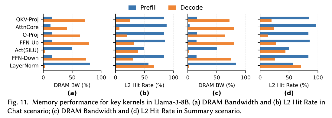
Diagram from Wang et al. Notice the high DRAM bandwidth and correspondingly lower L2 cache hit rate when the model is running in decode mode, demonstrating the higher memory intensity and lower arithmetic intensity of decode relative to prefill.
We can visualize this information in a different way in a roofline plot also created by Wang et al. The prefill phase is more compute bound and the decode phase is more memory bound. We can also see that the compute and memory intensity of each major component within prefill and decode also varies - this is not a uniform workload, even within a given stage.
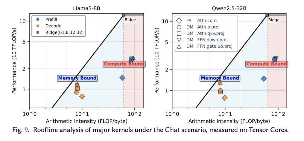
Source: Wang et al. Not only do prefill and decode have different arithmetic intensities, but different portions of each of those two phases vary in their arithmetic intensity as well.
The auto-regressiveness (and therefore high memory intensity) of the decode stage presents a problem for compute-heavy GPUs. It also creates an opening for SRAM-centric architectures, which excel at tasks with high memory bandwidth. This is why we see SRAM-centric chips focusing on inference, where their architecture gives them a fundamental advantage.
There's a strong precedent for treating prefill and decode differently. The authors of DistServe and Splitwise advanced the concept of prefill-decode disaggregation - splitting these two phases onto different pools of NVIDIA GPUs, so that they don't interfere with each other.
At Gimlet, we've extended that concept and built out a system to disaggregate the inference stages across accelerators from different vendors. This system is capable of doing things like mapping prefill to a high compute accelerator and decode to a high memory bandwidth accelerator, as well as finer-grained disaggregation schemes. NVIDIA is also moving toward heterogeneous disaggregation with its upcoming Rubin CPX product, which is optimized for high compute intensity workloads like prefill.

View of GPU pools running inference under 3 scenarios - aggregated inference on a unified pool, disaggregated inference across a single vendor pool, and disaggregated inference across accelerator pools from different vendors.
We're also starting to see more variation in disaggregation techniques than pure prefill/decode. For example, speculative decoders are an interesting target to disaggregate onto separate hardware. Speculative decoding aims to reduce the auto-regressiveness of the decode phase by running decode on a smaller model which produces "draft" tokens. These tokens are then verified in a compute-bound batch, which is a great fit for GPUs. Meanwhile, the speculative decoder model is small and memory-intensive, mapping well to SRAM-centric architectures because the weights fit more easily in SRAM.
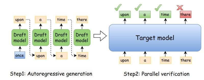
Image source. With speculative decoding, the large target model validates multiple tokens at once, so with an accurate draft model, one-by-one token processing by the large model can be successfully offloaded.
Each fragment of the workload - just like each hardware platform - has different characteristics and tradeoffs. For example, sparse and dense attention have different arithmetic intensities. Identifying the right places to subdivide the inference workload and running each slice of work on the most optimal hardware is our focus at Gimlet, and we are actively working with both traditional GPU providers and emerging SRAM-centric architectures to give our customers the best of both worlds within a single workload.
In an upcoming post, we'll share results from that work, disaggregating a single model across GPU and SRAM-centric hardware, including performance and efficiency comparisons across configurations.
Looking forward
As Xiaoyu Ma and David Patterson observed, LLM inference is in a crisis, primarily due to the challenges with decode. At the same time, demand for tokens is exploding, agentic workloads generate ~15X more tokens than traditional chat models, and frontier labs are under immense pressure to reduce end-to-end latency for users.
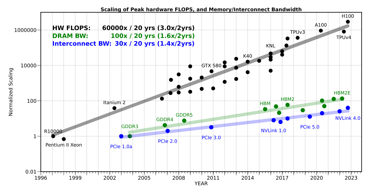
Source: Gholami et al. Compute is scaling faster than DRAM and interconnect bandwidth, creating a memory wall for LLM workloads.
This has created a perfect storm for near-compute memory chips (like today's SRAM-centric architectures), which provide superior performance for decode. We expect these chips will join GPUs as standard infrastructure for inference, and that the old world of running inference workloads 1:1 on a single hardware platform will end.
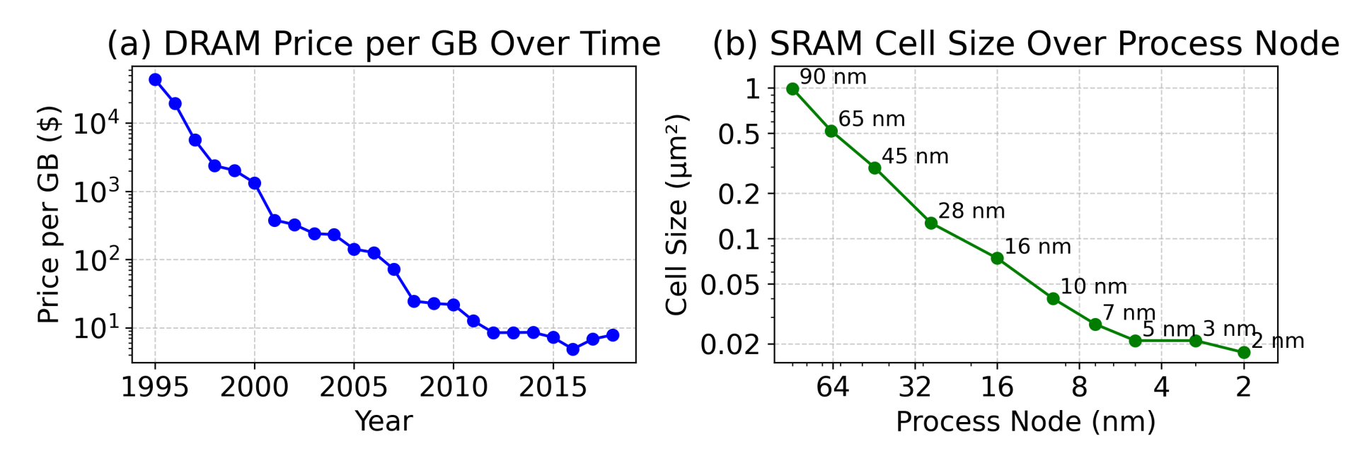
Source: Dayo et al. DRAM price per GB and SRAM cell size have both stalled.
We also predict this is the beginning, not the end, of hardware diversification, and specifically predict new solutions for both near- and far-compute memory. SRAM density has stalled, and DRAM cost per byte has plateaued, yet compute keeps scaling. To get around this crunch, the industry will need to better specialize memory architectures to workloads. HBM has historically served as a middle ground between SRAM and other forms of DRAM, but its dominance is being challenged from both sides. NVIDIA announced its Rubin CPX will use GDDR7 instead of HBM, which Semianalysis suggested was because prefill doesn't need HBM's bandwidth. From the other direction, d-Matrix's upcoming Raptor chip stacks custom DRAM directly on top of compute, which they claim offers 10X bandwidth over HBM4.
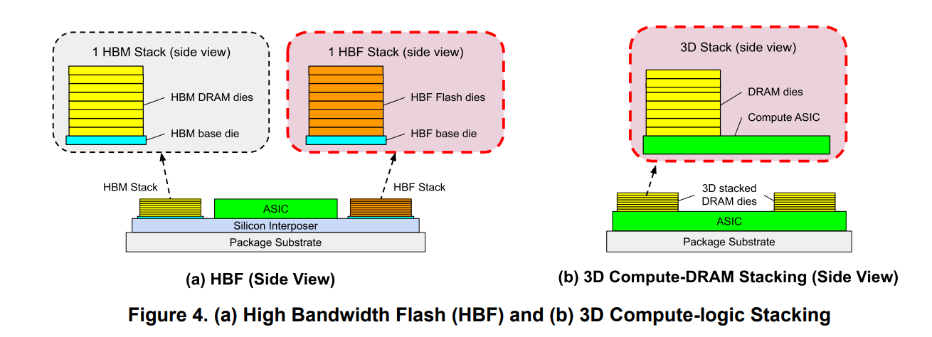
Source: Ma and Patterson. Memory stacking techniques like high bandwidth flash and on-compute stacked DRAM show promise for reducing LLM memory bottlenecks.
As we've seen, "SRAM vs HBM" is an implementation detail of a deeper decision: whether to place memory near or far from compute. Decode, with its large working set relative to reuse, is poorly matched to a traditional cache hierarchy. The solution is to support both extremes - massive amounts of memory, far from compute for some workload phases, or memory closer to compute for others.
In this new world of phase-specialized inference hardware, the question then becomes how to efficiently leverage that hardware at the software layer. That's the central problem Gimlet is focused on. Our multi-silicon inference cloud intelligently decomposes and executes inference workloads into fine-grained components, and is capable of running a single model across GPUs, SRAM-centric chips, and other accelerators.
As an industry, we are entering an exciting new era of chip design, with the unique demands of today's inference workloads pulling architectures in many different directions at once. We look forward to seeing (and using) the new chips that emerge under these constraints.